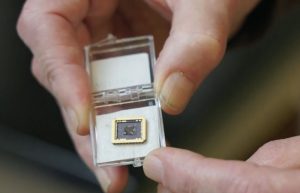
Researchers from the Georgia Institute of Technology have accomplished a historic feat by engineering the world’s first-ever functional graphene semiconductor.
In the 21st century, the quest for electronic devices that are smaller and faster has intensified, spanning applications in fields like medicine and robotics. Graphene semiconductors hold immense promise for advancing these technologies.
The drive to meet this escalating demand has spurred experts to focus on developing advanced materials for modern electronic devices.
Now, a team led by Walter de Heer, Regents’ Professor of Physics at Georgia Tech, has reached a significant milestone in this pursuit, creating the world’s first functional semiconductor using graphene.
“This feels akin to a Wright brothers moment,” remarked de Heer, highlighting the potential of this technology to propel advancements in quantum computing.
A promising silicon alternative
Graphene semiconductors, a two-dimensional carbon structure resembling a honeycomb, boast remarkable properties such as robust electrical conductivity, mechanical strength, and flexibility.
“It’s an extremely robust material, one that can handle very large currents and can do so without heating up and falling apart,” noted de Heer.
Semiconductors, crucial for electronic conductivity under specific conditions, are pivotal in modern electronics. The research was published in the journal Nature on January 3.
This innovation holds immense promise for the electronics industry, especially as the commonly used silicon material approaches its limits amid growing demands for faster processing and smaller devices.
Georgia Tech’s graphene semiconductor could potentially serve as a viable replacement for silicon in the foreseeable future read more. The semiconductor, compatible with conventional microelectronics processing methods, offers ten times the mobility of silicon and boasts unique properties.
“We now have an extremely robust graphene semiconductor with 10 times the mobility of silicon, and which also has unique properties not available in silicon,” emphasized de Heer.
The journey to material development
De Heer and his team achieved this breakthrough by pioneering a method to grow graphene on silicon carbide wafers using specialized furnaces. This process yielded epitaxial graphene—a single layer adhering to the crystal face of silicon carbide—demonstrating semiconducting characteristics upon extensive testing.
To evaluate the material’s conductivity, the scientists employed doping techniques. Their experiments revealed that the novel graphene semiconductor exhibits ten times the mobility of silicon.
Overcoming the band gap challenge
However, reaching this milestone was arduous; the team encountered a significant hurdle in graphene research—the absence of a “band gap”. This crucial electronic feature is essential for semiconductors to switch on and off effectively, fundamental to electronic performance.
“For years, graphene lacked the right band gap and couldn’t switch on and off at the correct ratio,” explained Lei Ma, director of Tianjin International Center for Nanoparticles and Nanosystems at Tianjin University in China.
Lei Ma, a co-author of the study, added, “Our technology achieves the band gap and is a crucial step in realizing graphene-based electronics.”
This big accomplishment marks a huge change in electronics. It’s bringing in a whole new time of technologies that use the amazing powers of graphene..